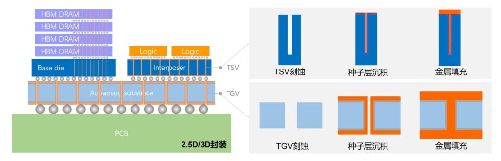
Advanced packaging represents a pivotal evolution in semiconductor technology, moving beyond the limitations of traditional scaling to enhance performance, power efficiency, and functional integration. It encompasses a suite of innovative techniques such as 2.5D and 3D integration, chiplets, and system-in-package (SiP) designs, which allow heterogeneous components—like processors, memory, and sensors from different process nodes—to be densely interconnected into a single, high-performance module. By focusing on the “how” of connecting dies rather than just shrinking transistors, advanced packaging enables the continuation of Moore’s Law, facilitating breakthroughs in artificial intelligence, high-performance computing, and IoT by creating more powerful and compact systems that were previously unattainable with monolithic chip designs.